Project Type: Research & Development
Applied Materials Unveils $5 Billion EPIC Semiconductor R&D Center in Sunnyvale, California
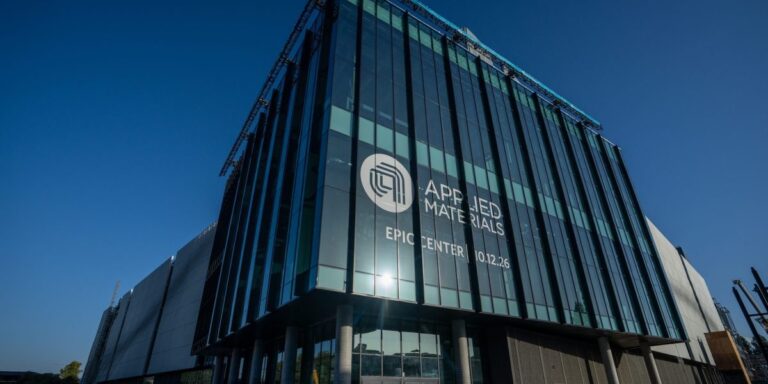
Applied Materials, Inc. unveiled on October 12, 2026 its Equipment and Process Innovation and Commercialization (EPIC) Center in Sunnyvale, California, a $5 billion capital investment in the world’s largest facility dedicated to collaborative semiconductor process technology and manufacturing equipment R&D.
Four acres of cleanrooms
The 600,000-square-foot structure houses nearly four acres of advanced cleanroom space and required more than six million construction hours to complete. It is designed to remove the hand-offs between materials research, equipment and process development and pilot production, speeding the path from invention to high-volume manufacturing.
Industry partners under one roof
Founding partners TSMC, Intel, SK hynix, Micron and Samsung Electronics are joined by innovation partners Broadcom, Advantest, SCREEN, KIOXIA and Besi, as well as research partners including Arizona State University, Rensselaer Polytechnic Institute and Stanford University.
Gary Dickerson, President and CEO of Applied Materials said:
“At EPIC, the world’s leading chipmakers, system designers, equipment partners and researchers will work side by side with our teams to accelerate the path from breakthrough materials innovation to high-volume manufacturing faster than ever before.”